In the previous article, we looked at the various losses incurred on the AC side of the circuit while charging an EV’s battery (from the breaker in the load center to the EVSE inlet on the EV), as well as things that could be done to minimize them, either by the OEM, the electrical contractor or the EV owner. This time our focus will shift over to the DC side of the circuit (and more specifically, the charger itself).
Regardless of where the charger is actually located—either onboard the EV or within a curbside DC fast charging station—a few basic functional requirements will be common to all chargers: provide galvanic isolation between the AC mains and the EV (i.e. have a transformer for isolation somewhere in the circuit); regulate and/or limit the current and voltage to the battery (i.e. be capable of constant current [CC] or constant voltage [CV] operation); and, more than likely, ensure the current waveform drawn from the mains is aligned in time and magnitude with the voltage waveform (in other words, perform power factor correction, or PFC). Unsurprisingly, there are numerous potential solutions to performing all three functions, but for the sake of not turning this article into a proverbial “Homeric catalog of ships,” we’ll just concentrate on the most common configurations—ignoring, for example, the use of a mains-frequency transformer for isolation, or so-called “single-stage” PFC and isolation converter topologies (which inevitably perform no function terribly well).
Basic requirements common to all chargers include: provide galvanic isolation between the AC mains and the EV; regulate the current and voltage to the battery; and perform power factor correction.
Assuming that isolation will be done with a high-frequency transformer, rather than a mains-frequency one, the first stage of the DC charger is the mains-frequency rectifier. For chargers that also do PFC—pretty much all of them these days—a bridge rectifier with a very small amount of filter capacitance (strictly to reduce noise and transients from the mains) will be used to produce sinusoidally-pulsating DC with a ripple frequency that is twice the mains frequency (i.e. 120 Hz for 60 Hz mains) and a peak value that is approximately 1.4x the RMS value of the mains voltage (~165 VDC for 120 VAC mains, or ~330 VDC for 240 VAC). The following PFC stage will then convert that pulsating DC to a much more smoothed-out DC with an average value close to 400 VDC, typically using a boost converter. Since the same DC bus voltage is produced regardless of the AC mains input voltage, this configuration is commonly described as universal input—meaning that the onboard charger can be plugged into either a 120 VAC or 240 VAC outlet without any action or concern on the part of the user to ensure things don’t blow up. Finally, there are the transformer isolation and CC/CV regulation functions, which are usually performed by a single converter. The most common converter topology used here is a full-bridge converter operating at a switching frequency of >50 kHz (typically in the range of 100 kHz-300 kHz, to be more precise) driving a high-frequency transformer. Control of the output current and/or voltage can be achieved by the conventional method of varying the duty cycle of each complementary pair of bridge switches from 0% to 50% (i.e. pulse-width modulation, or PWM), or through more exotic methods, like varying the phase shift of each pair from 0° to 180° (i.e. phase-shift modulation).

Series resonant full bridge converter:
(a) The topology of DBSRC; (b) The equivalent circuit of DBSRC.
Rectifying the AC from the mains into DC is usually done with four conventional silicon junction diodes in the bridge configuration. This puts two diodes in series with the mains at all times, and since every diode introduces a voltage drop while conducting (aka its forward voltage drop, or Vf), the humble bridge rectifier can exact a surprisingly large toll on overall charger efficiency. Diode Vf typically has a minimum value of 0.4 V to 1.8 V (depending on diode type and peak inverse voltage [PIV] rating) which also increases with current, both from simple (ohmic) resistance and a logarithmic factor of, typically, 60 mV/decade of current (also depending on diode type). Generally speaking, the faster a diode switches from conducting to blocking (i.e. its reverse recovery time, or trr) and the higher the PIV rating, the higher the initial Vf will be. Diodes operating at mains voltages and frequencies don’t need to be terribly fast, so a conventional Si pn junction type can be used with a trr of a few microseconds, but one shouldn’t be too stingy with the PIV, as the mains are a harsh place, filled with voltage spikes and transients—typically a 600 V PIV rating is the bare minimum for reasonable survivability, but there’s often little increase in Vf when going from 600 V to 1.0 kV or even 1.2 kV. With this combination of diode type and ratings, the Vf will likely end up at around 1.0 V at nominal rated current, so we’ll see a total drop of 2.0 V in the bridge rectifier. That’s a 1.7 percentage-point hit to efficiency at 120 VAC input right there! Some improvement can be had by going with a much higher current rating than is necessary—lowering ohmic and logarithmic losses—but getting to the mythical 0.6 V drop of a Si-junction diode at zero current ain’t happenin’.
Some improvement can be had by going with a much higher current rating than is necessary—lowering ohmic and logarithmic losses—but getting to the mythical 0.6 V drop of a Si-junction diode at zero current ain’t happenin’.
The next stage in the charger performs power factor correction, and this is usually done with a boost converter. In the boost topology, energy is stored in a choke when the switch is on, then some or all of that energy is released to the output capacitor via a blocking diode when the switch is off. It might seem counterintuitive, but at high power levels it is common to retain some energy in the choke from cycle to cycle (this is called continuous conduction mode, or CCM), because the peak and peak-to-peak (i.e. AC) currents are much lower than if the choke completely empties each cycle (called, unsurprisingly, discontinuous conduction mode, or DCM). In fact, the peak current in any of the power stage components when operating in DCM will be twice the average current, minimum, because current starts from zero every cycle. This not only exacerbates I2R losses throughout the power stage, it also incurs more AC losses in the choke, as they tend to be exponentially proportional to the peak-to-peak swing. However, the one huge disadvantage of CCM operation is that the blocking diode has to instantaneously switch from conducting forward current to blocking reverse current (it needs a trr of zero, in other words), which would normally mean using a Schottky type. Before the commercialization of SiC Schottky diodes, that was a non-starter, since the PIV rating of Si Schottkys tops out around 100 V, but SiC Schottkys have PIV ratings of 600 V and above, so they are the diode of choice here. They do have a higher Vf than their Si-junction counterparts (typically >1.8 V), but this has far less of an impact on overall efficiency than in the bridge rectifier, because there is only one of them in series with the relatively high voltage output (e.g. 400/401.8 = 99.55%). The other main points of optimization are the choke and the boost switch. In CCM operation, AC losses in the core and windings of the choke are less of a concern, so the focus should be on minimizing the DC (I2R) losses of the windings themselves (the converse is true for DCM—minimizing the AC losses then takes priority). For the switch, the obvious parameter to optimize is the on-resistance (RDS[ON]), but the less-obvious—and perhaps more important—parameter is the output capacitance (COSS), because this capacitance is charged up to the output voltage value every time the switch turns off, only to be discharged across the switch at next turn-on. This is an example of a loss that is both frequency- and voltage-dependent, and one that will covered in more detail next.
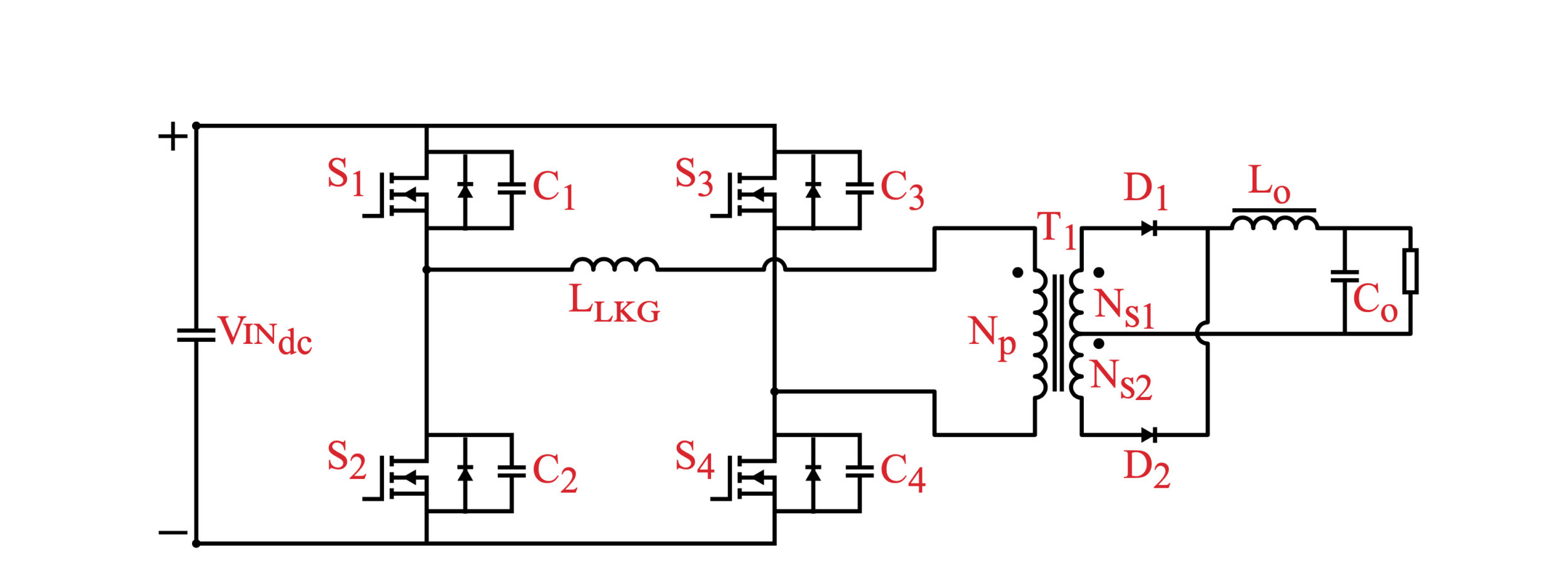
The final stage in the charger is usually a full-bridge converter which drives an isolation transformer, followed by a full-wave rectifier (with a choke-input filter if PWM is used to achieve CC/CV regulation). As with any switchmode converter, the higher the switching frequency, the smaller the magnetic and energy storage elements (transformers, chokes and capacitors), but, as was just hinted at above, increasing the switching frequency without bound is, well, bound to cause problems. In fact, switching losses routinely dominate in traditional “hard-switched” bridge converters above a switching frequency of 100 kHz or so, and the main contributors are the aforementioned charging/discharging of COSS, along with overlap of voltage and current during the transitions. A number of solutions for reducing—or even eliminating—switching losses are possible, with varying tradeoffs between reliability, complexity and flexibility (of, more specifically, the load range that can be accommodated while maintaining lossless switching), but broadly speaking, they fall into two categories: fully resonant and resonant transition (aka quasi-resonant).
Fully resonant converter topologies use resonant LC networks (aka tanks) to shape either the current, the voltage, or both waveforms into sinusoids.
Fully resonant converter topologies use resonant LC networks (aka tanks) to shape either the current, the voltage, or both waveforms into sinusoids so that the switches can be turned on (or off) at the moment the voltage (or current) passes through zero. This eliminates switching loss from overlapping voltage and current (if one parameter is zero, then the product of both is zero, of course), but the disadvantages of resonant converters are steep enough that they are infrequently used these days, because: (1) the resonant tank requires a certain amount of energy sloshing back and forth between its inductor and capacitor to function, either requiring a high minimum load or exhibiting terrible light-load efficiency; (2) this circulating current in the resonant tank incurs additional ohmic (I2R) losses from the various resistances in its path; (3) the only way to vary output power is by changing either the switching frequency or the pulse repetition rate, making compliance with EMI/RFI regulations more difficult; (4) when varying the frequency to effect regulation of the output, inadvertently crossing over the resonant peak will invert the control function, causing the output to collapse and, most likely, destroying the switches; (5) finally, the resonant frequency is dependent on the precise values of inductance and capacitance in the tank, and these are notoriously difficult to control in production volumes, possibly requiring hand-tuning of each unit.
The main solution to the downsides of fully resonant operation is to confine the resonant period to just the switching transitions, and one of the most popular ways to do this is to take advantage of the ringing that naturally occurs between the lumped sum of COSS from each switch in a bridge with the leakage inductance of the transformer. In hard-switched bridge converters, this ringing is a huge nuisance that requires dissipative snubbers (RC networks across each switch) to dampen it out so as to prevent failing EMI/RFI requirements. One of the most popular quasi-resonant topologies that uses the ringing between COSS and Lleakage is the phase-shifted full-bridge, and while discussing it in detail is beyond the scope of this article, those who are interested can look up Texas Instruments application note SLUA107A for more information. Regardless of the specific quasi-resonant technique employed, the current and voltage waveforms during the power transfer portion of each switching period will still be square—the same as in conventional hard-switched PWM—so peak currents and voltages will be the same as their hard-switched counterparts. Finally, because many quasi-resonant techniques utilize parasitic circuit elements for their operation, they can relax the need to minimize the leakage inductance of the transformer or the COSS of the switches, which usually translates into a lower cost for each of these often-pricey components.
Finally there are “wireless” chargers, which transmit power across an air gap from a coil in a base station to one in the EV. These chargers can be extremely convenient to use, but rarely exceed 80% transfer efficiency, and that’s before the other losses outlined above are factored in. Still, they seem to be gaining in popularity despite that, so they will be the topic of a future article. In the meantime, choosing SiC MOSFETs and a resonant transition converter topology for the charger are the two best ways to maximize its efficiency.
Read more EV Tech Explained articles.
This article appeared in Issue 58 – Nov/Dec 2021 – Subscribe now.