
In just the last few years there have been some major improvements in printed circuit board technology that are especially relevant to power electronics. Arguably the most important of the recent advances is the development of new board substrates that can withstand higher temperatures, along with metal cores for improved heat transfer, and the ability to selectively plate thicker copper onto specific traces, pads or planes for increased current-carrying capability only where it is needed. Getting the most out of these advances will require a deeper understanding of how boards are made in general, as well as working with board vendors and assemblers more closely than might normally be the case for plain vanilla designs.
Printed circuit boards (PCBs) are made from a wide variety of materials, but the most popular format when high reliability, insulation strength and temperature rating are required (but high RF performance isn’t) is FR-4, in which the substrate is a woven fiberglass cloth impregnated with epoxy. When the substrate is fully cured with copper foil laminated on the top and bottom (or just the top), then it is called a core; if the epoxy is not cured and there is copper on just one side, then it is called a prepreg, and is intended to be hot-pressed against a core to form a multilayer board. For example, a 4-layer board is typically constructed by hot-pressing a prepreg onto either side of a core. The pressure and heat cause the uncured epoxy in the prepreg to bond with the core and complete the cross-linking process that cures it. Most of the time you don’t have to worry too much about the exact details of how a board is made, but two notable exceptions are when you need predictable trace impedance (mainly in RF and high-speed digital), or a high dielectric strength between layers, because the ultimate thickness of the prepreg tends to be thinner than the core, and it is less consistent from board to board.
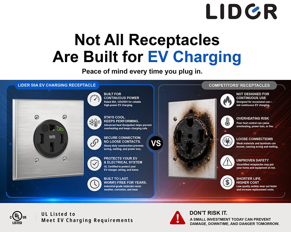
The two things that most limit the upper temperature rating of a PCB are the difference in coefficients of thermal expansion, CTE, between the copper and the substrate – which must be accommodated by the adhesive that joins the two – and the type of substrate. For example, the fiberglass cloth substrate in FR-4 can withstand far higher temperatures than any electronic component, but the epoxy resin can’t; thus, the temperature rating is entirely determined by the epoxy. The standard epoxy used in FR-4 has a glass transition temperature, Tg, of 130° C, which is where it goes from being stiff to substantially more flexible and, even worse, also experiences a dramatic increase in its CTE. Prolonged operation near, much less above, Tg will eventually result in board failure from cracked traces, vias being pulled apart, inter-layer shorts and even complete delamination of the copper from the substrate. Despite the fact that leaded solder requires heating to 225° C during infrared reflow soldering to fully wet the joints, problems with standard 130° C Tg FR-4 rarely occurred. When the Reduction of Hazardous Substances (RoHS) directives went into effect back in 2006, however, most electronic devices and sub-assemblies bound for the European Union had to switch over to lead-free solder, which invariably requires a higher reflow temperature – typically 255° C – and produces less reliable joints to boot. This mere 25° increase in reflow temperature was enough to trigger a massive increase in board/joint failures from straying too close (or even above) Tg, so new epoxy formulations were developed that increased Tg to 170° C. The poorer wetting and overall joint reliability of lead-free solder remains, so several product categories – including vehicles – are exempt from having to use it, and in this case the higher Tg can be used to advantage in allowing for prolonged operation near or above 100° C, something which can allow the higher-temperature-rated SiC and GaN semiconductors to be used more nearly to their full potential.
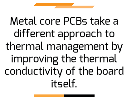
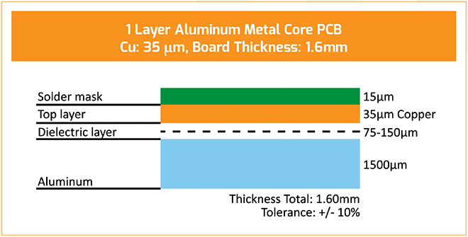
Metal core (more formally known as Insulated Metal Substrate) PCBs take a different approach to thermal management by improving the thermal conductivity of the board itself. This enables the board to transfer heat from components to the ambient more efficiently, reducing the size of additional heatsinks or even eliminating them entirely. As the name implies, a metal core board uses a metal plate as the core of the board rather than fully-cured FR-4. The metal plate is much thicker than the copper foil used for the traces – typically 0.8 mm (1/32”) to 1.6 mm (1/16”) – and is most commonly aluminum or copper. Since the metal core provides substantial rigidity, a very thin dielectric layer can be used between it and the copper trace layer(s) to provide electrical insulation at a much higher thermal conductivity than the equivalent thickness of fiberglass and epoxy in standard FR-4. The end result is a dramatic increase in thermal conductivity from a typical value of 0.25 W / m-K (watts per meter-Kelvin) for FR-4 to as high as 3 W / m-K for a single-sided metal core board. Note, however, that much of this benefit in improved thermal conductivity is lost in going to a double-sided board. Another potential gotcha is that the core itself is obviously electrically conductive, so it is more difficult to ensure good electrical isolation between it and component through-holes or vias. Some board manufacturers stack all the alternating layers of copper and dielectric film on one side of the core to maintain the low thermal resistance between the core and a heatsink and sidestep the via/hole insulation issue, but this comes at the expense of a higher thermal resistance between a heat-generating component (which will be on the outermost layer, of course) and the core. Thus, metal core PCBs are probably best reserved for relatively simple power electronics devices which don’t have to worry too much about signal integrity issues or maintain tight control over parasitic inductances and capacitances (such as LED lights, for one notable – and likely most popular – example).
Boards that can withstand higher temperatures or shed heat more efficiently are certainly welcome improvements to power electronics engineers, but the big Kahuna is the ability to carry more current for a given trace width, and that is what heavy (and “extreme”) copper PCBs deliver. The most common thickness of the copper in the finished board is 1 ounce per square foot, which corresponds to 35 um, respectively (or 1.378 mils per ounce weight). The ampacity of a trace is a function of area, allowed temperature rise, and whether it is on the surface or internal to a board. For external traces an empirically derived equation found in the PCB design directives document, IPC-2221A, is most commonly used:
Ampacity = 0.048 * dT0.44 * (1550 * A)0.725
Where dT is temperature rise in° C and A is area in mm2. A typical allowed temperature rise is 10 to 20° C, so an 8 mil (0.2032 mm) wide “signal level” trace on the external layer of a 1 oz board can handle around 0.75 to 1 A (DC or RMS), which is kind of impressive, really, for such a dinky trace. Bumping that up to 6.35 mm (250 mils) – which would be a typical width going to a pad on a TO-247 package semiconductor – only increases the ampacity to around 12.4 A, however, which rather starkly illustrates what a losing battle it is to rely only on trace width for ampacity.
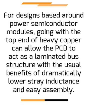
Hence the motivation behind the development of heavy and extreme copper boards, where “heavy” is typically defined as 4-20 oz / s.f. (0.14-0.7 mm thick) while “extreme” is anything above that (typically 100 oz / s.f., though one vendor goes up to 200 oz / s.f., or 7 mm thick!). For boards that mainly have TO-220 or TO-247 power devices, going up to 10 oz (0.35 mm) copper is most reasonable, as that boosts the ampacity of a 0.25” trace to 65.8 A, which is about as much as a TO-247 package device can handle, anyway. For designs based around power semiconductor modules (IGBT or MOSFET half-bridges and the like), going with the top end of heavy or even to extreme copper can allow the PCB to act as a laminated bus structure with the usual benefits of dramatically lower stray inductance and easy assembly (with a concomitant reduction in labor cost).
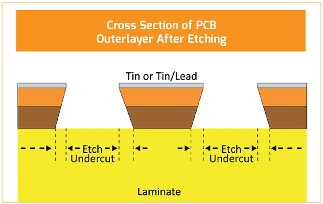
There are three ways to increase the thickness of the copper on a PCB: using a thicker foil for the blank board in the first place; plating additional copper onto the post-etched board; or plating additional copper onto just the traces and pads which actually carry high current. The first approach rapidly becomes untenable with increasing copper thickness: starting with a blank copper foil 0.7 mm thick (to say nothing of 7 mm!) then etching it down to the substrate to form individual tracks would take an uneconomically long time, and also result in severe undercutting of the traces. Consequently, plating more copper onto the already drilled and etched board would seem to be the preferred process, though the main caveat here is that copper will also deposit onto the side walls of the traces and plated-through holes, reducing the spacing between traces and potentially closing up the holes. Hence more generous “trace/space” rules are required with heavy and extreme copper boards.
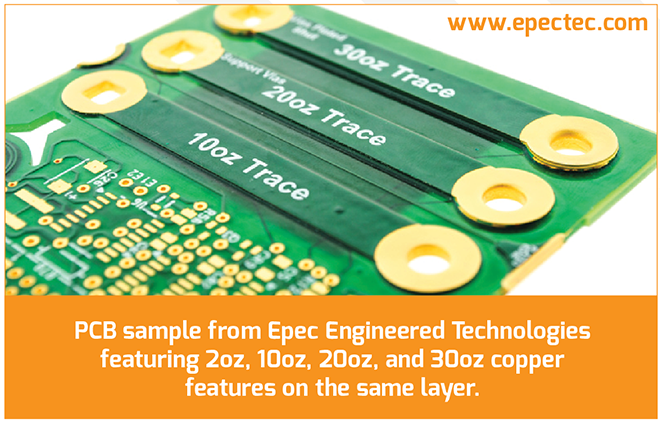
A related issue is that the minimum size for pads, traces and vias increases with finished copper weight, until it becomes impossible to accommodate smaller components (reliably, anyway). However, both of the aforementioned issues are ameliorated, if not eliminated, by selectively plating heavy copper onto only those traces which need it. Now a board can have, say, 10 oz copper for the power circuitry and 1 oz Cu for the support circuitry that needs to be in close proximity, such as gate drivers, feedback signal conditioning, etc. This sounds like an ideal solution, except for three major issues: neither PCB CAD software, solder paste stencil printers, nor pick-and-place machines have ever had to contend with different copper thicknesses on one board before. Depending on the CAD software and P-n-P machine it might be possible to kludge your way around this, but there’s no good way to use a standard stencil printer to apply the solder paste, which means applying it dot by dot, one pad at a time. A final downside is the price of selective heavy copper (and, to a lesser extent, standard heavy/extreme copper): at least one board vendor warns that the cost might be unpalatable for all but military and aerospace applications, which is generally a huge red flag for the rest of us. Still, the potential reduction in assembly labor (except for solder paste application), along with improved heat dissipation and tighter integration of power and support circuits could (eventually) outweigh the higher cost of selective heavy/extreme copper to the point that it is compelling even for the infamously cost-sensitive, such as automotive suppliers.
Read more EV Tech Explained articles.
This article appeared in Charged Issue 45 – September/October 2019 – Subscribe now.