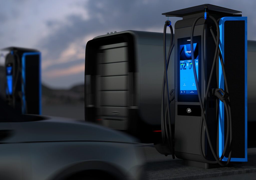


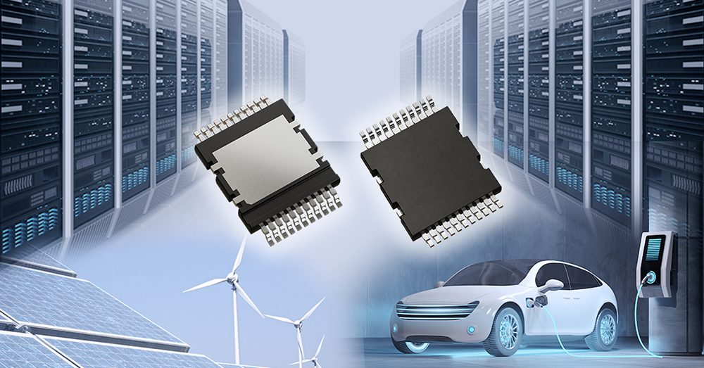
Toshiba has started shipping test samples of the TW007D120E, a 1,200 V trench-gate SiC MOSFET designed for power supply systems in high-power applications, including EV charging stations, energy storage, AI data centers and photovoltaic inverters.
The device is built around Toshiba’s proprietary trench-gate structure, which embeds gate electrodes directly in etched trenches in the semiconductor substrate rather than placing them on the surface. Toshiba says the architecture achieves lower on-resistance per unit area than planar SiC MOSFETs, reducing conduction losses while simultaneously cutting switching losses.
Compared to Toshiba’s third-generation SiC MOSFET (the TW015Z120C), the TW007D120E reduces RDS(on) per unit area by approximately 58% and improves the RDS(on) × Qgd figure of merit—the standard measure of the conduction loss/switching loss trade-off—by approximately 52%.
The headline specs: 1,200 V drain-source breakdown voltage, 172 A continuous drain current at 25° C case temperature, and a typical RDS(on) of 7.0 mΩ at VGS = 15 V. Gate-drain charge Qgd is 33 nC and total gate charge Qg is 317 nC, both at VGS = 15 V.
The device uses a low gate drive voltage of 15-18. V. It ships in the QDPAK package with top-side cooling, which supports higher power density by moving heat out through the top of the device rather than the board.
Toshiba aims to begin mass production in fiscal year 2026, and says it will expand the lineup into automotive applications.
Source: Toshiba Electronic Devices & Storage



















 EV Engineering Webinars & Whitepapers




 EV Tech Explained