


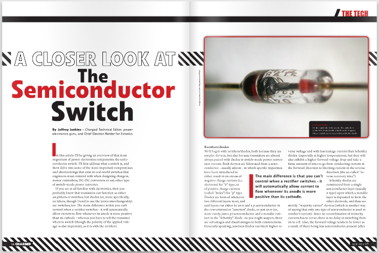
In this article I’ll be giving an overview of that most important of power electronics components: the semiconductor switch. I’ll first address what a switch is, and then delve into some of the more important compromises and shortcomings that exist in real-world switches that engineers must contend with when designing chargers, motor controllers, DC-DC converters or any other type of switch-mode power converter.
If you are at all familiar with electronics, then you probably know that transistors can function as either amplifiers or switches, but diodes (or, more specifically, rectifiers, though I tend to use the terms interchangeably) are switches, too. The main difference is that you can’t control when a rectifier switches – it will automatically allow current to flow whenever its anode is more positive than its cathode – whereas you have to tell the transistor when to switch (though the polarity of the applied voltage is also important, as it is with the rectifier).
Rectifiers/diodes
We’ll begin with rectifiers/diodes, both because they are simpler devices, but also because transistors are almost always paired with diodes in switch-mode power conversion circuits. Both devices are fabricated from a semiconductor – usually silicon – in which specific impurities have been introduced to either result in an excess of negative charge carriers (i.e. electrons) for “n” type, or of positive charge carriers (called “holes”) for “p” type. Diodes are formed whenever two different layers meet, and said layers can either be an n and a p semiconductor in the conventional or “junction” diode, or just an n (or, more rarely, just a p) semiconductor and a metallic contact in the “Schottky” diode. As you might suspect, there are advantages and disadvantages to both constructions. Generally speaking, junction diodes can block higher reverse voltage and with less leakage current than Schottky diodes (especially at higher temperatures), but they will also exhibit a higher forward voltage drop and take a finite amount of time to go from conducting current in the forward direction to blocking current in the reverse direction (the so-called “reverse recovery time”).
Schottky diodes are constructed from a single semiconductor layer (usually n type) upon which a metallic layer is deposited to form the other electrode, and thus are strictly “majority carrier” devices (which is another way of saying that only one type of semiconductor is used to conduct current). Since no recombination of minority carriers has to occur, there is no delay in switching from on to off. Also, the forward voltage tends to be lower as a result of there being less semiconductor present (after all, the very name “semiconductor” implies less conductivity than a conductor-like metal). The primary downsides of the Schottky construction are much higher capacitance (which can mimic the effect of slow reverse recovery), a limited ability to block reverse voltage, and a higher leakage current for a given reverse voltage. One recent, but prominent, exception is the Silicon Carbide (SiC) Schottky. SiC has a “wide bandgap,” which basically means it takes more electrical “force” to move an electron across the semiconductor. Regular silicon has a bandgap of ~1.1 electron-volt (eV) while SiC has a bandgap of ~3.2 eV. In other words, a SiC diode can block ~3x the voltage for a given die thickness, and since SiC also has a higher thermal conductivity and can tolerate a higher operating temperature, it can handle a lot more current for a given die area, as well. Of course, TANSTAAFL1 applies, and SiC diodes (and MOSFETs) are significantly more difficult to fabricate, and therefore cost a lot more, but their unique advantages often eliminate the need for costly (and bulky) snubbers or larger heat sinks, so the overall design can end up costing less while delivering better performance and taking up less space.
Transistors
Among the various types of transistor, the two types most commonly used in EVs are the Metal Oxide Field Effect Transistor (MOSFET) and the Insulated Gate Bipolar Transistor (IGBT). These two devices share many characteristics and can even be used interchangeably at times, but there are several key differences between them that exert a profound influence on which device is most appropriate for a given application.
Conventional wisdom is that MOSFETs are preferred in low-voltage and/or high-switching frequency applications because they – like Schottky diodes – are majority carrier devices and thus can switch very rapidly. But at the same time the lack of assistance from minority carriers means conduction losses increase rapidly with blocking voltage (approximately a square function). In contrast, IGBTs are preferred at higher voltage/higher power applications where a high switching frequency is neither desirable nor practical because they use both majority and minority carriers (i.e. both electrons and “holes”) to conduct current and thus can handle much more current for a given die area. But the need to recombine the minority carriers at turn-off results in a much longer turn-off time and thus limits the practical switching frequency.

A Power MOSFET made by Fairchild Semiconductor (Image courtesy of alsteele/Flickr)
The conventional wisdom oversimplifies things a bit, but the broad distinction between the two technologies holds true (even factoring in the higher blocking voltage capability of the new SiC MOSFETs). This is best illustrated by comparing the specs of an actual MOSFET and IGBT selected from an online parts distributor catalog, sorting by increasing resistance for the MOSFET and increasing forward voltage for the IGBT, and then picking the first device in each list. Both devices will be rated for 600 V and come in a common TO-247 plastic package, whose maximum dissipation will be limited to 60 W, as that is about the most heat this package can shed without resorting to exotic cooling measures (big nota bene here – don’t expect the leads on a TO-247 package to carry more than 50-55 A, regardless of how effective the heat sink is; those current ratings that claim over 100 A are more intended to reflect a low forward voltage drop or on-state resistance).
The MOSFET with the lowest on-state resistance at the time of the sorting is Fairchild part number FCH76N60N, which costs about $26 in single quantities. It has a typical on-state resistance of 28 mΩ at 25 C, but that rises with temperature to 38 mΩ, so it’s good for 40 A at 60 W of allowed dissipation with a reasonable heatsink. The typical switching times are downright blistering at 44 ns for turn-on and 48 ns for turn-off using the recommended minimum value of gate resistance (you can always increase the transition times by using a higher gate resistance, but reducing gate resistance below the minimum can result in destructive oscillations).

An IGBT Module made by Mitsubishi Electric (Image courtesy of Thomas Lok/Flickr)
The 600 V IGBT with the lowest forward voltage drop of 1.36 V is IXYS part number IXGX72N60A3H1, which costs less than half as much as the MOSFET at about $12 in single quantities. It can even handle a slightly higher current of around 44 A for the same dissipation, but as promised, the price paid for lower conduction loss is a higher switching loss: rise time is still plenty fast at 34 ns, but fall time stretches out to a leisurely 250 ns, or about 5x slower than the MOSFET. And there is nothing the design engineer can do to make this IGBT turn off faster: the recombination time for the minority carriers is strictly a function of the way the IGBT is constructed (however, the turn-on time can be controlled by the gate resistance value, same as the MOSFET).
So you wouldn’t want to use the Fairchild MOSFET in a motor controller, because the faster a voltage is switched the more capacitively-coupled AC current will flow, and this AC current causes dielectric losses in the winding insulation (which wasn’t designed to be a capacitor!) and erosion of the bearings. In addition, a high switching frequency will result in higher “iron losses” in the motor (which increase at approximately the 1.6 power to frequency). Conversely, the IXYS IGBT wouldn’t be the best choice for use in a “hard-switched” DC-DC converter or charger, as the long turn-off time (and consequent high turn-off energy) would demand a lower switching frequency, which in turn means larger magnetic components (inductors and transformers) and capacitors.
There are other factors that have to be considered when choosing between IGBTs and MOSFETs, and one of the biggest gotchas with the latter is the so-called anti-parallel “body” or “intrinsic” diode that is automatically formed alongside the MOSFET. The body diode seems like a win-win because you need an anti-parallel diode across each switch to conduct reactive current in an AC motor controller or a bridge converter, to give two examples. Unfortunately, the body diode in a MOSFET is slow to turn off, because it suffers the same recombination process that plagues the IGBT and it has a huge area – the same as the MOSFET itself – relative to what a discrete diode with the same voltage and current rating would otherwise require. Also note that the reverse recovery time (which is roughly equivalent to the fall time in an IGBT) increases with voltage rating. In fact, the reverse recovery time (trr) of the body diode in the Fairchild MOSFET is listed as 200 ns, that effectively means it is almost as slow as the IGBT, because when the reverse recovery time of a diode is longer than the turn-on rise time of the switch it is paired with, the switch suffers increased losses from having to deal with what is effectively a short-circuit across the input supply, and the peak current during such time will only be limited by the stray inductance and resistance of the circuit. In contrast, an anti-parallel diode must be specifically added to an IGBT, so it can be optimized both for area and recovery time (that said, note that the anti-parallel diode in the IXYS IGBT has a trr of 140 ns, which is quite a bit slower than the turn-on time of the IGBT at ~35 ns, but IXYS probably figures – rightly so – that you won’t want to turn on the IGBT in 35 ns when it will take 250 ns to turn it off).

Of course there are always the exceptions that prove the rule, and recent improvements in both IGBT and MOSFET technology are blurring the lines between the two devices. The aforementioned SiC MOSFET – though still a device that only uses majority carriers – can carry almost as much current per unit area as an IGBT with the same blocking voltage (though this arguably has more to do with SiC tolerating a much higher junction temperature and having better thermal conductivity, rather than higher conductivity). Another fairly recent innovation is the “Super Junction” MOSFET, which can exhibit 2-3x lower on resistance for a given blocking voltage, but it has a much more complicated structure, so it is still more expensive than an IGBT of similar current/voltage rating (the SJ MOSFET will still switch faster, though).
Improvements in IGBT technology have been more incremental over the past few years, but one new fabrication process, the “Non-Punch-Through” construction, has dramatically lowered the thickness of the silicon wafer required to make an IGBT without a reduction in blocking voltage. On-state voltage drop does increase, but it has a positive temperature coefficient at higher current, so multiple NPT devices in parallel will share current better. Turn-off time and short-circuit ruggedness are also much improved over the traditional IGBT fabrication process (now called “Punch-Through”) and that latter attribute has resulted in NPT IGBTs becoming the first choice for a semiconductor switch in motor controllers at the 100 kW+ power level, pretty much totally displacing older – and difficult to control – thyristor technology.
Read more EV Tech Explained articles.
This article originally appeared in Charged Issue 13 – APR 2014 – Subscribe Here.