
A previous article examined loss mechanisms in traction motors, which tend to be the single biggest source of losses in a modern EV drivetrain. This time, the focus is on the various power semiconductors, as they are the next biggest source of losses. Also covered in brief are ways to mitigate these losses and design decisions that can avoid them in the first place.
The major power conversion devices in an EV are the charger, inverter and DC-DC converter, and, as is the case with the traction motor, it is difficult to nail down an average efficiency level for any of them, because they all operate at wildly different power levels. Also, as with the traction motor, some losses are fixed regardless of load, while others are linearly or exponentially proportional to load.
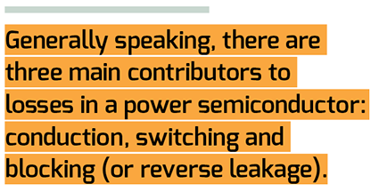
Generally speaking, there are three main contributors to losses in a power semiconductor: conduction, switching and blocking (or reverse leakage). In some cases these losses can be ignored, but most of the time they will sneak up and bite you in the proverbial posterior if not addressed. Further complicating matters is that too aggressively trying to minimize switching losses by switching faster can lead to worse problems with overvoltage and EMI (electromagnetic interference). As Robert A. Heinlein famously quipped (and instantly coined the mantra for engineers the world over): TANSTAAFL, or, “There Ain’t No Such Thing As A Free Lunch.”
Conduction losses are simply the product of the current flowing through a switch or diode when it is forward biased (i.e. – turned on) and the voltage drop across it. The problem is determining what the actual voltage drop is at any given time, because this changes with temperature and current. Bipolar transistors (including IGBTs) and Schottky diodes (including SiC types) behave like a diode in series with a small resistance when forward biased. As with all diodes, there is a minimum forward voltage that must be applied before conduction occurs, and this forward drop can span the range of 0.3 V for a low-voltage Schottky diode to 2.2 V for a 1,700 V IGBT or SiC diode. The temperature coefficient of the diode is also negative (typically -2 mV / ° C), but that of the effective series resistance can be positive or negative depending on the device and specific construction. MOSFETs, in contrast, behave like a simple resistor when turned on, albeit one with such a strong positive temperature coefficient that on-resistance, RDS[on], typically doubles going from 25° C to 125° C. Regardless, you can get a reasonable first-pass estimate of the effect on-state drop will have on efficiency by simply subtracting the worst-case datasheet value from the supply voltage, keeping in mind that bridges (including the half-bridges in inverters) put two devices in series. So an inverter using IGBTs that drop 1.6 V will subtract 3.2 V from the supply, and if the supply is 320 V, that cuts efficiency by one percentage point right there.
Schottky diodes are renowned for having a lower forward drop, but at around the 60 V rating, the advantage goes back to conventional pn diodes, so only choose the Schottky if you need the speed. This also applies to SiC Schottkys, though the difference in forward drop is much less dramatic…except when it comes to the anti-parallel diode in SiC MOSFETs: typical values for this diode are around 3.2 V (!), compared to the 1.8 V or so of a discrete part (both rated for 600-650 V and 1-20 A). As mentioned above, IGBTs and other bipolar devices have a minimum forward drop regardless of how low current is, so light-load efficiency can be much worse in an IGBT-based design. For example, the minimum voltage drop of a 600 V / 50 A IGBT will be in the range of 0.8 to 1.0 V at 1 A, while the on-resistance, RDS[on], of a similarly rated 600 V MOSFET might be around 50 mΩ, so only dropping 50 mV at 1 A. However, the voltage drop across the IGBT will only increase by 60 mV per decade of current, plus a tiny bit more from the intrinsically low effective resistance, so at 50 A the IGBT might lose 1.7 V, versus at least 2.5 V for the MOSFET.
Losses incurred from leakage current when the device is supposed to be off are another potential source of misery for the unwary engineer, though they are much more easily avoided if one doesn’t tempt fate by operating the device at high temperatures and/or close to its rated voltage. Once again, pn junction diodes have the advantage over Si-barrier Schottkys, though the gap is not quite so wide for SiC types. A couple of comparisons between a conventional and a Schottky diode will illustrate this best. The ubiquitous 1N4001 pn junction diode allows 5 uA of leakage at 25° C and 50 V, increasing to 50 uA at 125° C; a 10x increase to be sure, but still only amounting to 2.5 mW of additional dissipation. In contrast, the popular SS15 Schottky leaks 400 uA at 25° C – already 80x more than the 1N4001 – and this increases to a whopping 6 mA at 100° C, or 15x higher still! This results in an increased dissipation of 0.3 W, which is certainly not negligible for a device this size. Things look better for the SiC Schottky at 600 V, however: the high-speed pn junction STTH4R06 rated for 600 V / 4 A has 25° C / 125° C leakage currents of 3 uA / 30 uA, respectively, while its SiC counterpart, a C3D04060E, lets through 25 uA at 25° C but a still-tolerable 100 uA at 175° C (and note that 175° C rating!); so, 60 mW of additional loss, worst-case, which can be safely ignored in a diode this size.
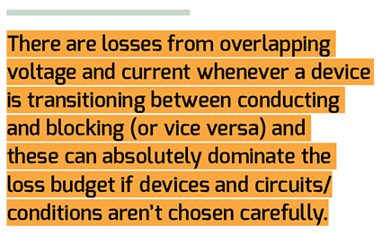
Finally, there are losses from overlapping voltage and current whenever a device is transitioning between conducting and blocking (or vice versa) – that is, switching – and these can absolutely dominate the loss budget if devices and circuits/conditions aren’t chosen carefully. Unlike conduction and blocking losses, however, it is entirely possible to eliminate switching losses with appropriate circuit techniques, but at a cost in complexity, and perhaps, in reliability as well, but more on that later.

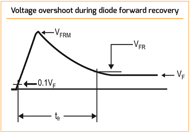
Let’s start with a loss mechanism that almost no one thinks about: forward recovery in diodes. Any engineer that designs switchmode converters becomes very familiar with reverse recovery – which is the time it takes for a diode to go from conducting to blocking current – but less well-appreciated is the fact that it often takes time for pn junction diodes to go from blocking to conducting, and even more surprising is that forward recovery is often slower than reverse recovery in “fast” diodes! The main penalty incurred by forward recovery is increased loss in the diode, because during that time the voltage across it will overshoot the “nominal” Vf spec by anywhere from a few hundred mV to volts, if the dI / dt (rate of change in current) is high enough. Forward recovery never used to be specified in datasheets, but it is starting to show up more and more as its ill effects in switchmode converters become more widely known and appreciated; the aforementioned STTH4R06 has a forward recovery of 100 ns with an overshoot of 5 V at a dI / dt of 100 A / us (somewhat perversely, the datasheet gives a reverse recovery overshoot current of 7.5 A at 200 A / us, but reverse recovery times of 50 A and 100 A / us, making it difficult to make a fair comparison). Still, the 20 W of peak power lost (i.e. 5 V * 4 A) seems terrible, but when averaged out over, say, a 10 us period (i.e. 100 kHz), this amounts to about 0.2 W of additional loss. The opposing switch also has to contend with this additional voltage, but that typically won’t matter unless the switch is only rated for 20 V or less.
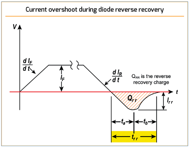
While forward recovery might be safely ignored in a pn junction diode, reverse recovery usually cannot; the exception is when load or circuit conditions allow the current through the diode to go to zero before the opposing switch next turns on. This is because the diode effectively acts as a short circuit during reverse recovery, and if the switch turns on into a short circuit, a huge spike of current will flow through it and the diode. Another issue is that this spike of current can excite ringing between the various stray L’s and C’s that are inevitably present (such as junction capacitance, discussed next), and somewhat perversely, faster diodes are more likely to be guilty of this. So you get higher losses and EMI-radiating ringing as a bonus! To calculate reverse recovery losses, multiply the amount of charge (in Coulombs) lost per cycle by the voltage and frequency to get watts. Some datasheets give you the reverse recovery charge, Qrr, directly, but if only given reverse recovery time and peak current, then a reasonable estimate of Qrr is trr * Irr / 2. One final point about reverse recovery: the anti-parallel (aka “body”) diode in non-SiC MOSFETs is really slow, so it has terrible reverse recovery losses. Normally this diode won’t be faced with a situation where it is conducting right up until an opposing switch turns on, but one notable exception that has burned many an engineer is the phase-shifted full-bridge converter (if you’re curious, look for a paper by Alexander Fiel and Thomas Wu on this subject).
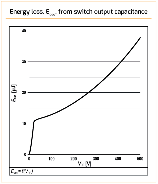
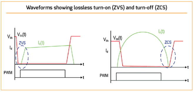
While Schottky diodes don’t suffer from either forward or reverse recovery, both Schottkys and MOSFETs do tend to have a much higher capacitance across their active junction than similarly rated bipolar devices, and this capacitance can act exactly like reverse recovery…go figure. Junction capacitance, referred to here as Cj, can only affect the circuit when the device is off/reverse biased, obviously, and because it is a property of the electric field in the semiconductor, it is inversely proportional (though non-linearly) to the applied reverse voltage. Aside from changing value with voltage, Cj behaves like any other capacitor, so it passes alternating current in proportion to frequency and voltage, and stores energy in proportion to voltage squared. The current that flows through Cj is usually irrelevant – even an old, high-current Schottky with a Cj of 2 nF at 15 V will shunt less than 20 mA at 100 kHz (compared to a 40 A current rating) – and it doesn’t heat up the device as true reverse leakage current does. However, the energy stored by Cj is a very relevant cause of losses (and sometimes even outright failures) in MOSFETs, because it gets charged up to the bus voltage (or higher) every time the switch turns off, only to dump that charge right back into the switch the next time it turns on. For example, a state-of-the-art MOSFET such as the IPW60R018 has an effective Cj (or Coss in the datasheet) of 361 pF at a drain voltage swing of 400 V, so it stores 28.8 uJ of energy each cycle (in fact, this very spec is also given in the datasheet as Eoss). At a switching frequency of 100 kHz, that’s 2.89 W of additional loss right there. That might not sound like much, but it will absolutely cook a TO-247 package device like this if it isn’t mounted on more than a token heat sink, and note that this loss applies regardless of actual load current. However, it is possible to eliminate this loss entirely by using one of the myriad “quasi-resonant” zero-voltage switching, or (QR-)ZVS, schemes. Basically, an external inductor is used to form a resonant tank with Cj so as to shape the voltage swing across the MOSFET into a half-sinusoid, then only turning on the MOSFET after the voltage reaches zero. It’s fairly simple in concept but often somewhat tricky to get working right, and ZVS is invariably lost at very light loads, as sufficient current must flow through the inductor for it to store enough energy to ring down the voltage across Cj.
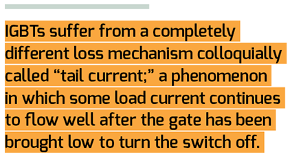
IGBTs tend to have much lower Cj values than their similarly powerful MOSFET counterparts, so ZVS doesn’t really help them. Instead, they suffer from a completely different loss mechanism colloquially called “tail current;” a phenomenon in which some load current continues to flow well after the gate has been brought low to turn the switch off. The physical process behind tail current is similar to that of reverse recovery in pn diodes: it takes time to sweep all of the minority carriers (that reduce conduction losses) out of the junction. Various techniques can be used during manufacture of the IGBT die to dramatically reduce (but not eliminate) tail current, but they all increase conduction losses and/or decrease ruggedness (namely, the ability to tolerate a short circuit). However, there is a complementary scheme to ZVS in which the current waveform is shaped into a half-sinusoid and the switch is turned off at zero current (no prizes for guessing what this scheme is called). It should be noted that turn-on of the IGBT in ZCS is still lossy, just as turn-off of the MOSFET is in ZVS, but these transitions are much more benign for their respective devices. Absent using such quasi-resonant schemes – which are difficult to the point of being impractical in the traction motor inverter, by the way – a good rule of thumb is to select a switching frequency such that switching losses are approximately equal to conduction losses. Of course, if audible noise from switching is either tolerable or unlikely to be heard – such as in the inverter – then it can make a lot of sense to lower the switching frequency to further reduce losses (though that does require a larger input capacitor).
Finally, try to have realistic expectations for the efficiency of things: to go from 90% efficiency to 95% you have to cut losses in half, after all, which does sort of put things into perspective.
Read more EV Tech Explained articles.
This article appeared in Charged Issue 42 – March/April 2019 – Subscribe now.