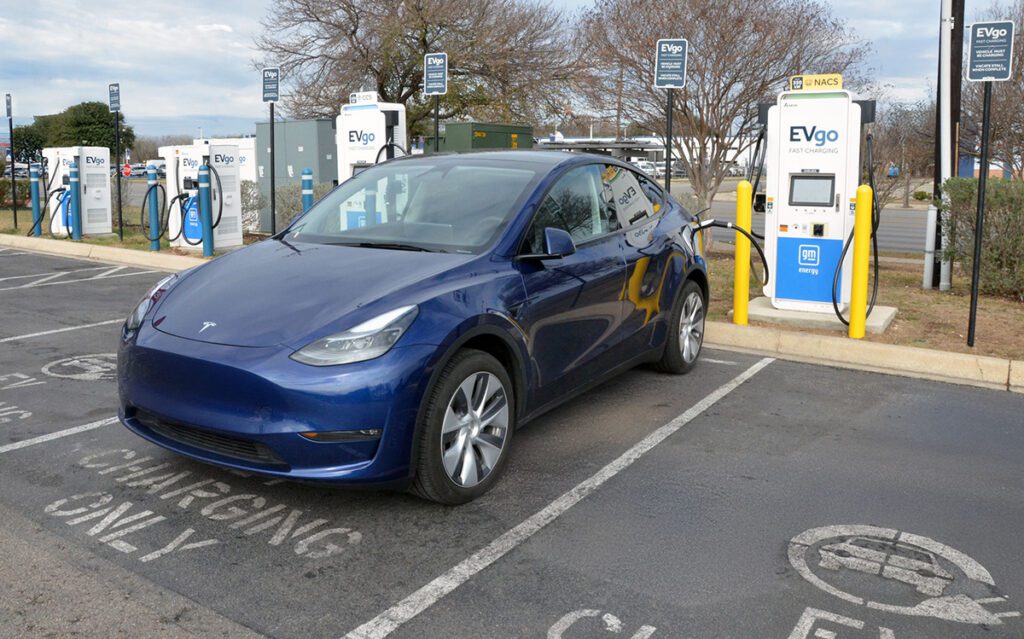
Incorporating robust circuit protection in electric vehicles ensures reliability and safety
By Jim Colby, Littelfuse, Inc.
Designing circuits for the next generation of automotive innovations is extremely challenging. New vehicle designs incorporate a plethora of complex microprocessor circuitry as well as the latest in EV onboard charging technologies. To ensure today’s new designs are robust, safe, and can withstand overloads, transients, and electrostatic discharge, electronics designers must be sure their circuits have the necessary components to prevent this damage. This whitepaper addresses seven mission-critical onboard charging circuits, providing recommendations for both circuit protection and efficient power control.
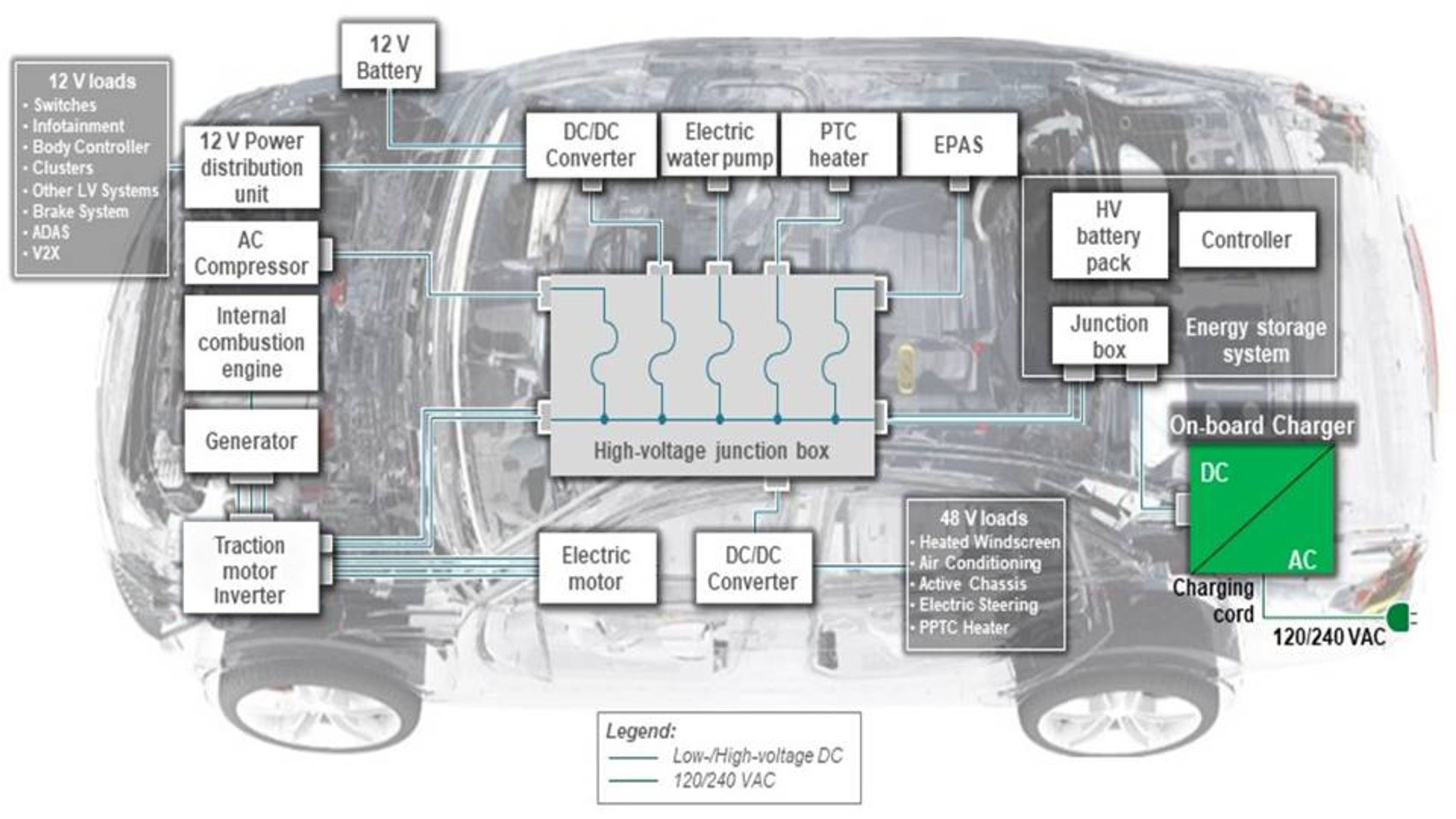
An overview of the major circuits of an electric vehicle is illustrated in Figure 1, above. This diagram describes a hybrid vehicle that incorporates an internal combustion engine and an electric drive. Hybrid vehicles represent a worst-case scenario for electronics engineers who must develop circuitry hardy enough to withstand the transients that can be generated by both the internal combustion engine and the high-power electric motors.
In addition to protecting these circuits from transients inherent in EVs, the onboard charger must also contend with the AC power line, which has the potential for generating both transients and overloads. The onboard charger’s circuits should be protected in the same way the design engineer would protect any line-powered product. Communication circuits must also be properly protected to ensure the processors survive any ESD transients, and so that data corruption is avoided. Furthermore, engineers will want to design this circuit to minimize internal power consumption, which helps the battery charge time to be as short as possible.
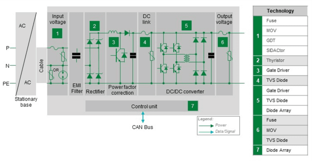
Onboard chargers convert the AC line voltage into the DC voltage required for charging the main battery pack. The pack can have a fully charged voltage in the range of 300–500 volts. Today’s EV consumers want faster charging. As a result, higher power charging circuits are needed that include three-phase power. An example onboard charger block diagram with a single-phase circuit is shown in Figure 2. Each circuit block identifies the recommended protection components and, where needed, the control components that optimize the charger’s efficiency.
1. Input Voltage
The input voltage section is susceptible to transients, including lightning strikes and surges on the AC line. A fuse that provides overload protection is the first line of defense. Consider fuses with a high interrupting current rating and a high voltage rating; this ensures the fuse will open under the worst-case current overload. Place a metal oxide varistor (MOV) just downstream of the fuse to protect against a surge transient or a lightning strike. MOVs absorb the transient energy and help prevent it from damaging the other circuits that are further downstream. If the onboard charger uses three-phase power, consider adding MOVs for both phase-phase transient protection and phase-neutral transient protection.
For even greater protection of the downstream circuits, place a bipolar thyristor in series with the MOV. Thyristors have a very low clamping voltage, typically around 5 V. Use of a thyristor also enables the designer to select an MOV with a lower standoff voltage. The net effect of this combination is the reduction of the peak transient voltage to which the downstage circuitry is momentarily exposed.
A gas discharge tube (GDT) provides the fourth level of superior circuit protection. The GDT provides high-resistance, electrical isolation between the hot and neutral lines and the vehicle’s chassis ground. GDTs provide an additional level of protection against fast-rising transients from lightning disturbances.
2. Rectifier
Circuit designers can select rectifier block thyristors with sufficient current handling capacity to supply the necessary power for fast, high power charging. Usage of this technology (over rectifier diodes) provides a “softer” start (lower in-rush current) and reduces electrical stress on the Power Factor Correction block. Thyristors also safely absorb surge current transients that may have passed through the input voltage and EMI filter stages.
3. Power Factor Correction
The efficiency of the charge is improved by the power factor correction circuit, which reduces the total power drawn from the AC power line. Use a gate driver and an insulated gate bipolar transistor (IGBT) to control the amount of inductance in the circuit. Be sure to select a gate driver with a sufficient operating voltage range for control of the IGBT. Also, consider selecting a gate driver with high immunity to latch-up and with fast rise and fall times to quickly switch the IGBT. Fast rise and fall times, combined with a low supply current, improve the circuit’s power efficiency. Be sure to protect the gate driver from ESD by selecting a gate driver with built-in ESD protection or adding an external ESD diode. Bi-directional or uni-directional ESD diodes can withstand as high as 30kV ESD transients.
4. DC Link
The DC link is made up of the capacitor bank that stabilizes the ripple generated by the high-power DC/DC converter. Design engineers concerned about large voltage transients reaching the DC link can utilize a high voltage TVS diode to protect the capacitor bank.
5. DC/DC Converter
The DC/DC section steps up the output charge voltage and generates the charge current for the battery. Similar to the Power Factor Correction circuit, the DC/DC converter requires a robust gate driver. If a gate driver selection does not include internal ESD protection, be sure to add an ESD diode to protect the gate driver. The addition of an external ESD diode does not degrade the performance of the gate driver.
It is important to make sure that the power IGBTs are protected from voltage transients. In addition to protection from external transients, the IGBT creates turn-off switching transients due to L·di/dt effects from internal parasitic inductance. Place a TVS diode between the collector and gate of each IGBT to eliminate the potential damage to an IGBT from this transient. The TVS diode reduces the di/dt of the current transient by raising the gate voltage. When the collector-emitter voltage exceeds the breakdown voltage of the TVS diode, current flows through the TVS diode into the gate to raise its potential. The TVS diode continues to conduct until the transient is eliminated. Known as active clamping, use of a TVS diode as a collector-gate feedback element keeps the IGBT in a stable state. There are some IGBTs that have built-in active clamping TVS diodes. Select either that type of IGBT or add TVS diodes to the circuit. For more information on active clamping, reference the application note.1
6. Output Voltage
Current overloads and in-vehicle voltage transients can occur when motors turn on and off or when current is instantaneously interrupted by a break in a cable. For this reason, the output voltage stage requires robust protection. Consider employing a fuse to protect from an overcurrent resulting from a short in the battery pack or in the cables that carry the battery voltage. An MOV or a TVS diode protects against any potentially damaging voltage transients.
7. Control Unit
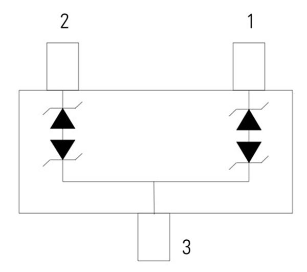
The charger’s control unit communicates with the data network via the CAN bus. To avoid damage to the communication circuits and avoid data corruption, be sure to provide ESD and transient protection. This protection can be implemented with a single, space-saving component. For example, Figure 3 shows a dual-line TVS diode array designed for CAN bus signal lines protection. TVS diode arrays designed for protecting communication lines have minimal capacitance and do not degrade the transmitter/receiver I/O states.
By following these recommendations for protection and control, design engineers can be assured their new onboard charging systems will have robust, reliable, and safe circuits for their electric vehicle consumers. Whenever possible, remember to use AEC-Q qualified components that have been certified for use in hazardous automotive environments (i.e., AEC-Q101 covers discrete semiconductors and AEC-Q200 covers passive components such as varistors). It’s important to remember that you can also take advantage of the manufacturers’ expertise and wealth of application knowledge for assistance when selecting appropriate protection and power control components.
To learn more, download the Automotive Electronics Applications Guide courtesy of Littelfuse, Inc.
Additional References
1 Application Note: Using High Voltage TVS Diodes in IGBT Active Clamp Applications. 2020.
2 Shaping the future of E-mobility with Littelfuse solutions. (June 2020)


