Designing high-voltage power conversion systems today is both more challenging and more convenient than it has been in the past. More challenging because the demands of efficiency and power density require the use of the most bleeding-edge technologies available. More convenient because those advanced technologies, necessary to put into service, often include integrated features that reduce the engineering involved.
The on-board charger is the perfect example of the challenges and conveniences of high-power design. This system has a clear goal to meet the needs of future automobile models. It must deliver higher power, perhaps at a higher voltage, than the previous version. It also must do this with reduced weight. After all, what’s the point of charging a larger battery if the extra energy goes into carrying the charger around?
For power FETs, the latest technology to produce the highest efficiency in a power converter system is Silicon Carbide (SiC). SiC FETs are able to withstand the high voltages involved in on-board charging applications while delivering high power. They do this with less losses due to ambient temperature changes while switching faster than previous technologies. Fast switching means that there is less loss in the switching action, and that the size of magnetics is reduced.
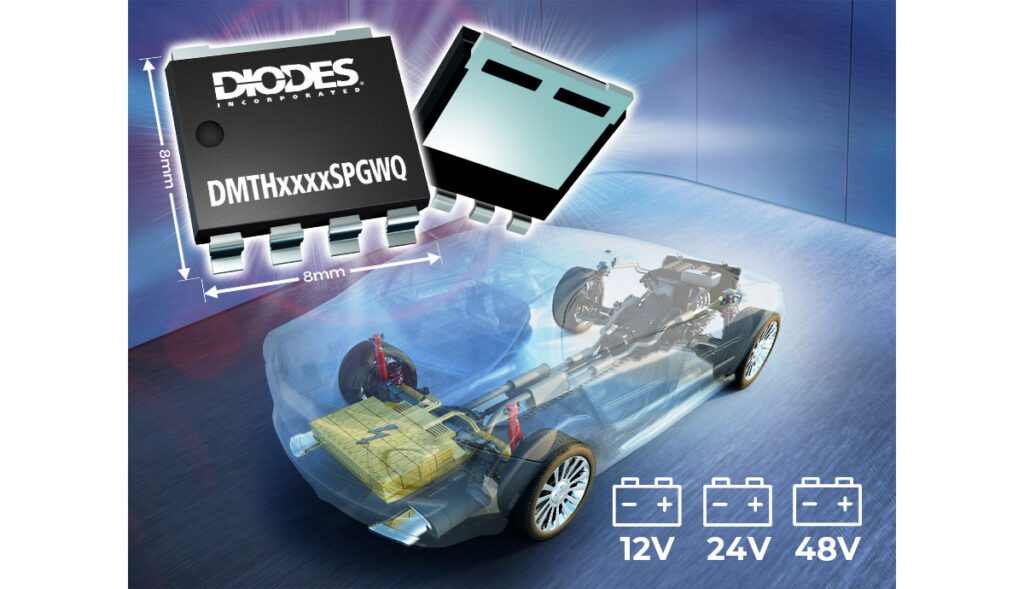
Today, implementing SiC technology is made convenient by the use of multi-FET packs. These implement 2 to 6 FETs in a single package. Often, they also contain additional functionality such as an integrated temperature sensor or diodes to facilitate particular switching architectures. FET packs that facilitate quick and easy creation of half-bridge switching stages are the most popular.
Besides being convenient, there are distinct advantages to having multi-FET packs when designing a power conversion system. The integration provides a great opportunity for system size reduction and the optimized pinout and package of the module reduces layout considerations to relatively common PCB best practices. Also, the thermal management is made more convenient—only a single heat sink is needed for the entire FET pack. The tighter connection between FETs improves efficiency and reduces parasitic inductances overall.
With all the challenges that go into the realization of a complete system, it can be daunting to take advantage of the convenience of a SiC FET module. The FET pack module provides the switching components for half-bridge and other switching architectures, but much more has to be considered to use the components to their full capabilities.
Today, manufacturers of isolated gate drivers offer reference designs that include all the components necessary for efficient drive of FET modules, but building these reference designs is a challenge to overcome in order to evaluate the benefits of a FET module. Some FET module vendors offer complete evaluation boards with pre-selected combinations of components, but due to the unique requirements of FET modules in specific applications, these evaluation boards are often too limiting. Luckily, some manufactures of isolated gate drivers like Silicon Labs have begun to create interchangeable all-in-one gate driver boards that can be used with a wide range of FET modules.


