


Samsung Electronics has developed a silicon carbide-free graphene coating that it says could immediately double the capacity of lithium-ion batteries. That would be an impressive feat indeed, considering that capacity has increased only twofold since Li-ion batteries were first commercialized in 1991.
Many researchers are investigating the potential of silicon as an anode material, but it suffers from poor cycle life. Samsung’s new process creates a sort of protective layer around the silicon to make battery life longer. When paired with a commercial lithium cobalt oxide cathode, the coating allows the cell to reach volumetric energy densities almost two times higher than those of current commercial Li-ion batteries.
In “Silicon carbide-free graphene growth on silicon for lithium-ion battery with high volumetric energy density,” recently published in the journal Nature Communications, a team from the Samsung Advanced Institue of Technology (SAIT) describe how they developed the technology of direct graphene growth over silicon nanoparticles without silicon carbide formation.
Son In-hyuk of SAIT said, “This observation suggests that the two-dimensional layered structure of graphene and its silicon carbide-free integration with silicon can serve as a prototype in advancing silicon anodes to commercially viable technology.”
The SAIT team fabricated the anode material by growing graphene directly on a silicon surface while avoiding silicon carbide formation by developing a chemical vapor deposition process that includes CO2 as a mild oxidant. The graphene-coated silicon nanoparticles reach a volumetric capacity of 2,500 mAh cm−3, which the team says is the highest value reported to date for any Li-ion battery anodes, while exhibiting excellent cycling and rate performance.
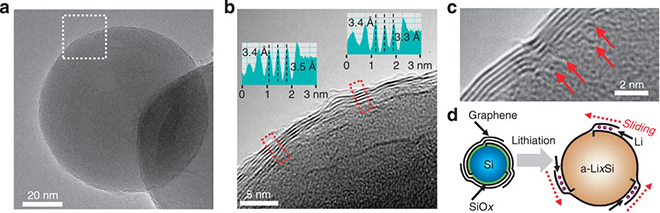
(a) A low-magnification TEM image of Gr–Si NP. (b) A higher-magnification TEM image for the same Gr–Si NP from the white box in a. (Insets) The line profiles from the two red boxes indicate that the interlayer spacing between graphene layers is ~3.4 Å, in good agreement with that of typical graphene layers based on van der Waals interaction. (c) A high-magnification TEM image visualizing the origins (red arrows) from which individual graphene layers grow. (d) A schematic illustration showing the sliding process of the graphene coating layers that can buffer the volume expansion of Si. Source: Son et al.
The graphene layers anchored onto the silicon surface use a novel approach to accommodating the well-known problematic volume expansion of silicon: a sliding process between adjacent graphene layers. This allows the designers to avoid providing a void space in the electrode to accommodate silicon expansion.
Industry watchers said the technology may be available for actual products in two or three years.
Source: Green Car Congress, Korea Bizwire
Image: TechStage (CC BY-ND 2.0)