


Just as engineers are starting to get used to the advantages (and quirks) of silicon carbide (SiC ) devices, another semiconductor material joins the fray: gallium nitride, or GaN. Though there are some superficial similarities between these two materials, and even some overlap in their areas of best use, it is my opinion that only one of them is going to see widespread application in EV power converters such as chargers, inverters, etc.
SiC and GaN are both classified as wide band-gap and compound semiconductor materials. The latter classification just means they are comprised of different elements, and is all but irrelevant here, but the wide band-gap classification does have profound implications for device behavior and performance. This is because the term band gap basically describes how difficult it is to get a material to conduct electricity without having to ionize it first (that is, turn it into plasma). More specifically, it is a measure of the amount of energy (given in electron-volts, or eV) that it takes to promote an electron in the outermost valence of an atom to what is called the conduction band (hence the term band gap). The band-gap energy of metals is effectively 0 eV, so they are good conductors – electrons can easily pop out of the outer valence to the conduction band or vice versa – whereas materials with a band-gap energy of around 4 eV or higher are considered to be insulators. Materials with a band-gap energy between those two extremes are, of course, considered semiconductors, with an approximate value of 1.14 eV for Si, 2.3 to 3.3 eV for SiC and 3.4 eV for GaN.
It might appear, then, that wide band-gap materials like SiC and GaN are at a disadvantage compared to Si simply because they are much closer to being insulators than conductors. While it is true that a SiC or GaN device with a given die area and thickness will exhibit a higher bulk resistivity (and therefore on-resistance) than a comparable Si device, the wider band gap means their dice can be much thinner for the same voltage rating. The thinner dice have lower on-resistance, and lower thermal resistance too. Another related advantage to a wide band gap is that leakage current starts off lower and increases much more slowly with a rise in temperature (in more technical terms, the spontaneous generation of charge carriers from heat is reduced). These materials can also withstand higher operating temperatures (even if their die attach solder or packaging can’t!), which, when combined with the lower leakage and thermal resistance, means they can handle a lot more power for a given device size.
While GaN really is a new material for any kind of use, starting with blue LEDs in the late 1980s, SiC has been used as an abrasive for over a century (in this context, it’s also referred to as carborundum), and it even had a brief stint as the crystal detector in early radios, followed by use in yellow, then blue, LEDs (until GaN supplanted it). GaN is entirely man-made, but SiC can be found in nature as the mineral moissanite – but good luck finding any, as it only forms under the same extreme conditions that produce diamonds. GaN has roughly the same thermal conductivity as Si-based semiconductors, while SiC is over twice as good at conducting heat (slightly better than copper, in fact). SiC also has a relatively low thermal coefficient of expansion, which makes it less prone to damage from high temperatures and thermal cycling. All in all, SiC seems like an ideal semiconductor material, but there is one catch: it can form a bewildering array of crystal structures (called polytypes), each of which has slightly different physical properties, including the all-important band-gap energy. Unsurprisingly, this can make producing SiC semiconductor devices a bit of a challenge, but as manufacturers gain more experience with the vagaries of this material, they should continue to improve yields and lower pricing.
That said, SiC still commands quite a premium over similarly-rated Si parts, so it is best deployed where there is no Si equivalent, such as 1,200 V MOSFETs with drain-source resistances under 200 milliOhms or 600 V to 1,200 V Schottky barrier rectifiers, especially in high-power-boost power factor correction converters, in which any time spent in reverse recovery by the output diode generates considerable losses, as well as increased stress on the boost switch. GaN is really too new to address on an economic basis – a perusal of Mouser’s website shows just 14 parts in stock at the time of this writing – but switches made from it command an even higher premium than does SiC for the same voltage and current rating.

Whether a premium in price is worth it depends on the advantages a particular technology delivers, and the value proposition for SiC, at least, is very compelling, especially for devices rated 650 V or higher. Sure, there are the “SuperJunction” Si-MOSFETs that can achieve very respectable on-resistance values in the 600 V to 900 V range, but at 1,200 V there is simply no comparison anymore: SiC blows away Si, and manufacturers are even now rolling out 1,700 V rated parts, which Si doesn’t even try to compete with. GaN should be capable of a similar voltage rating vs conduction loss figure of merit, but the GaN switches available so far seem to be rated for 650 V or lower. GaN can switch much faster than SiC or Si – 10 ns rise/fall time, with minimal turn-on/turn-off delays, too – but this may be a problem masquerading as a solution, as switching 300 V or more this rapidly results in massive amounts of ringing, voltage overshoots and RFI/EMI. The RFI/EMI issue may very well be insurmountable when practical considerations such as, say, passing electromagnetic compatibility (EMC) testing is are factored in. The wise (or the battle-scarred) know that nothing ruins a development schedule and budget quite like failing EMC testing so badly that you have to do a total mechanical and electrical redesign.
There are other peculiarities of each of these new materials that can also trap the inexperienced (or unwary). The first is the difference in behavior of the intrinsic (aka “body”) diode that is found in both Si and SiC MOSFETs (but not in GaN switches). This diode is a pn junction type formed as a consequence of the way these modern vertical-structure power/switching MOSFETs are constructed. The body diode is infamous for being slow in the Si-MOSFET – taking 300 ns or longer to turn off – so engineers learn to set up circuit conditions so that it either does not ever conduct, or at least, does not have to endure high dV/dt when reverse voltage is reapplied. The body diodes in SiC MOSFETs are considerably faster, however, with reverse recovery times that would give a hyperfast discrete pn diode a run for its money (60 ns or less). One might naively assume that there’s no need to worry about reverse recovery losses (or outright failure) from body diode conduction in the SiC MOSFET, but take a closer look at the forward voltage spec in the datasheet and you’ll likely rethink that assumption: 2.5 V to 3.5 V (or more)! As a result, overall losses might be higher than expected when using SiC MOSFETs in circuits in which body diode conduction is inevitable (such as bridge and two-switch forward or flyback converters). Other than that one caveat, SiC MOSFETs (and Schottky diodes) are compelling choices, especially when operating at high bus voltages (>600 V) and/or temperatures (>100° C).
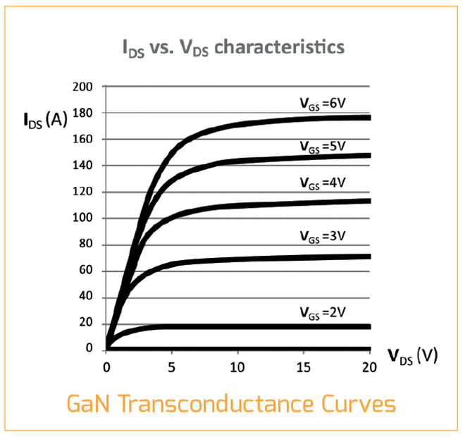
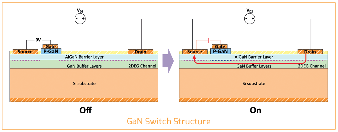
In contrast, GaN definitely has some gotchas to watch out for, and this technology is just too new for most engineers to have had any experience with it. Complicating matters is the fact that different structures have been employed to make GaN switches with equally different functional (and pathological) behaviors. The first thing to note, though, is that GaN switches are not MOSFETs, even though they use the same terminal names and behave similarly (though not exactly the same, as we’ll soon see). In fact, the first GaN switches (formally referred to as HEMTs, for High Electron Mobility Transistors) had more in common with JFETs as they operated in depletion mode – that is, they were normally on with 0 V applied to the gate – and the gate would conduct significant current if forward-biased too much, leading to device destruction. Depletion mode operation is intrinsically unsafe in most power converter circuits for the obvious reason that one generally doesn’t want their switches to be turned on by default, but to enable enhancement mode operation requires building the GaN switch on top of a silicon substrate (to incorporate a control MOSFET). This complicates the manufacturing process, but it results in a switch that power electronics engineers will at least consider using.
Although GaN switches don’t have a body diode, they will still conduct current in the reverse direction when off, and with a diode-like characteristic, except that the voltage drop is the sum of the gate threshold voltage and the voltage biasing the gate. Note, then, that biasing the gate with a negative voltage will increase the voltage drop during reverse conduction! Since negative gate bias is practically a requirement for reliable operation of IGBTs and MOSFETs at high power, in order to counteract spurious turn-on via the “Miller” capacitance (that is, the parasitic capacitance between the gate and drain terminals), this can be quite a gotcha, indeed. GaN switches do exhibit much lower parasitic capacitances overall – a major reason they are so fast – but they also have a relatively low gate threshold voltage compared to Si or Si-C MOSFETs (and IGBTs have higher thresholds still). Whether the reduction in Miller capacitance is sufficient to counteract the lower threshold (and faster switching speed) will likely have to be evaluated on a device-by-device basis, and, while slowing the switching speed down will also help, that sort of eliminates the primary reason for choosing GaN over any other technology.
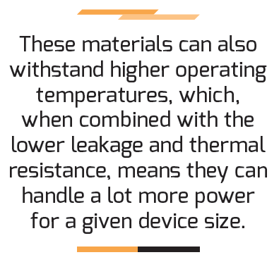
Finally, GaN switches are very particular about how their gates are driven, though the current generation is much improved in this respect compared to the first devices that were made commercially available in 2010. The biggest issue is that there isn’t much margin between the threshold and maximum allowed voltages for the gate, the latter being 6 to 10 V, depending on the manufacturer. Also, the current through the drain-source channel is strongly dependent on gate voltage – much more so even than in IGBTs, and also way more so than in MOSFETs. This could be a plus or a minus in that deliberately under-driving the gate will limit fault current – much as the desaturation mechanism in IGBTs does – but this results in higher conduction losses overall, which, again, defeats one of the reasons for selecting GaN in the first place. In the end, SiC is plenty fast enough for any power conversion application in an EV, and its overall higher ruggedness is a real plus, too. GaN is really too fast for its own good here, and seems better positioned to applications in which space is at a premium, and where MHz switching speeds can actually be used, for example in low-voltage DC-DC converters.
Read more EV Tech Explained articles.
This article appeared in Charged Issue 43 – May/June 2019 – Subscribe now.


