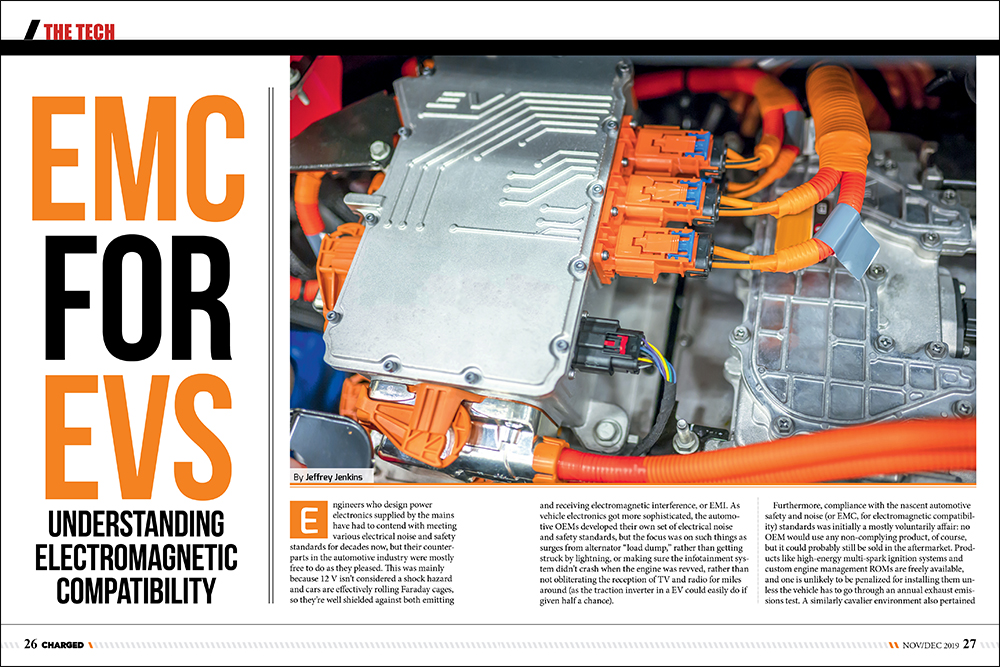
Engineers who design power electronics supplied by the mains have had to contend with meeting various electrical noise and safety standards for decades now, but their counterparts in the automotive industry were mostly free to do as they pleased. This was mainly because 12 V isn’t considered a shock hazard and cars are effectively rolling Faraday cages, so they’re well shielded against both emitting and receiving electromagnetic interference, or EMI. As vehicle electronics got more sophisticated, the automotive OEMs developed their own set of electrical noise and safety standards, but the focus was on such things as surges from alternator “load dump,” rather than getting struck by lightning, or making sure the infotainment system didn’t crash when the engine was revved, rather than not obliterating the reception of TV and radio for miles around (as the traction inverter in an EV could easily do if given half a chance).
Furthermore, compliance with the nascent automotive safety and noise (or EMC, for electromagnetic compatibility) standards was initially a mostly voluntarily affair: no OEM would use any non-complying product, of course, but it could probably still be sold in the aftermarket. Products like high-energy multi-spark ignition systems and custom engine management ROMs are freely available, and one is unlikely to be penalized for installing them unless the vehicle has to go through an annual exhaust emissions test. A similarly cavalier environment also pertained to OEM EVs in their early years, but it was only a matter of time before the safety and EMC regulations that applied to mains-powered equipment were adapted for EVs. So far it appears that complying with the safety standards is relatively straightforward (these standards are developed by committee, after all), but for many engineers, achieving EMC compliance still seems to involve more dark art and mystic incantation than science. That’s not true, of course – it just seems that way most of the time.
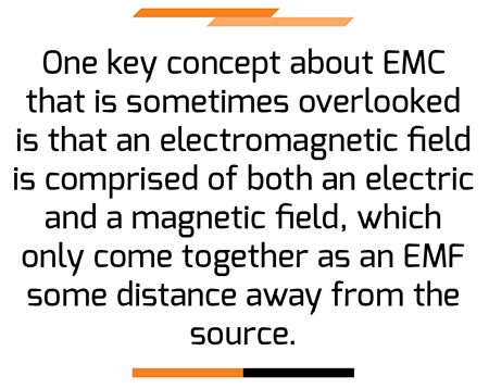
One key concept about EMC that is sometimes overlooked is that an electromagnetic field, or EMF, is comprised of both an electric (E) and a magnetic (H) field, which only come together as an EMF some distance away from the source (and, for a bit of trivia, with a fixed V/I relationship of 377 Ω). The distance at which this combining occurs is not formally defined, but is usually considered to be 1-3 λ (wavelengths). Closer in (aka the “near field”), one or the other will dominate depending on circuit conditions: E-fields arise from fast changing voltages (high dV/dt) while H-fields result from fast changing currents (high dI/dt).
As with many complex problems, there is an overwhelming desire to look for a simple explanation or solution (echoing H.L. Mencken here), and in the case of EMC issues, that would arguably be: don’t make accidental antennas. While this is certainly true, it’s not particularly actionable advice all on its own, as almost anything conductive can be turned into an antenna, and even some things you wouldn’t think could cause any problems can become the biggest headaches of all, such as a seam in a metal enclosure! A more useful, albeit still general, set of guidelines would be:
- Minimize the loop area of any conductors (wires, traces, bus bars, etc) which handle high dI/dt or are low-impedance.
- Minimize the surface area and/or shield any conductors that experience high dV/dt or are high impedance.
- Don’t switch any faster than you need to for reasons of data rate (digital logic) or efficiency (power conversion).
- Any hole, slot or seam in a conductive surface can become an antenna, too.
Not adhering to the first bullet point is the one that seems to cause the most problems, though it is sometimes unavoidable when equipment grounding requirements are factored in (forming the dreaded “ground loop” – a case in which the safety regulations often conflict with the EMC ones, unfortunately). Minimizing loop area simply means keeping the forward and return pathways for any circuit as close together as possible, and this applies to everything from CAN bus and Ethernet cables to battery wiring to the bus plates in an inverter. In all cases the point is to get the magnetic fields of the forward and return pathways to cancel each other out, which reduces both the emission and reception of H-field noise.
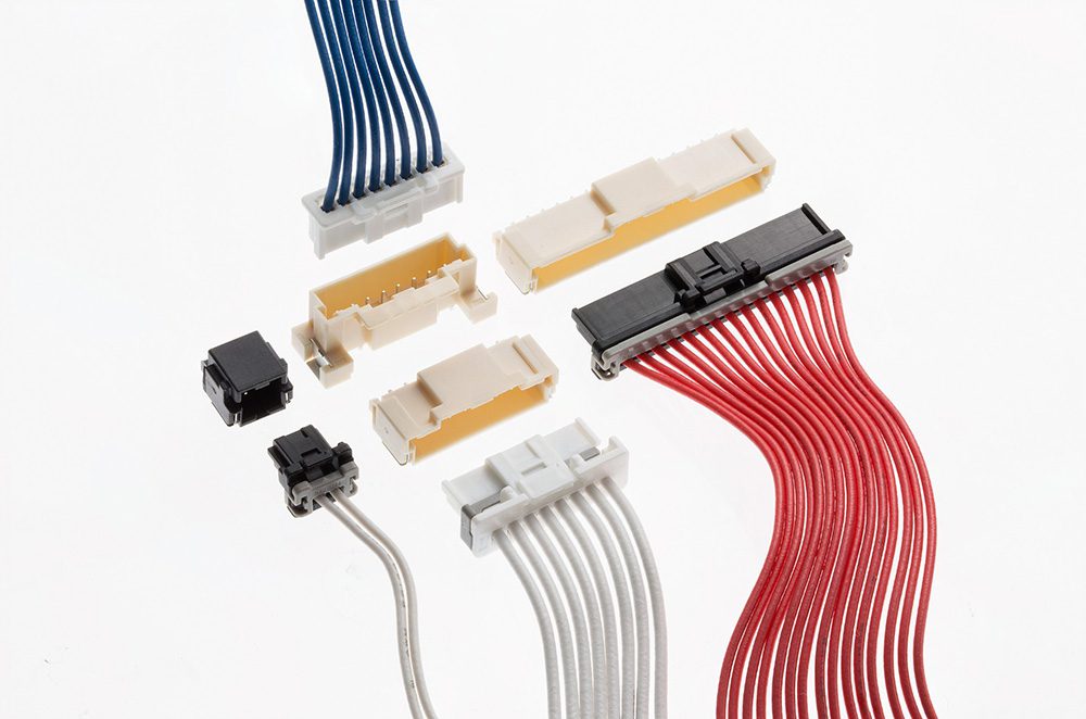
In the specific case of CAN and Ethernet, twisted-pair cable is most commonly used because it ensures each wire has the same overall magnetic environment, so that any external H-field noise is induced on each wire equally; the noise is common-mode, in other words. Differential signaling – driving equal but opposite polarity currents on each wire of the pair – then ensures that the H-fields produced by the wires will cancel each other out nearly completely, preventing noise emission and crosstalk. This combination – differential signaling and ensuring all induced noise is common-mode – allows for excellent rejection of noise by the receiver even at high data rates and over long distances. When signals are single-ended and distances aren’t too long – for example, board-to-board interconnects – then a ribbon cable with every other wire dedicated to ground/common can work nearly as well as twisted pair. In this case every signal conductor (except for the outer two) is surrounded by a return conductor, so suppression of both the emission and reception of H-field noise is quite good, but if it isn’t quite good enough, then adding a ferrite “clamp core” across the cable will usually suffice (those cylindrical lumps often seen on round multi-conductor cables represent precisely that solution, in fact).
The same principle of placing the forward and return conductors in close proximity can be applied to PC boards by dedicating an entire layer to ground/common, and in bus structures by using plates with a large surface area separated by a thin insulator instead of individual bus bars (aka a “laminated bus structure”). In both applications, high-frequency (high dI/dt) currents will automatically mirror themselves in the planar conductor surfaces, which tremendously reduces noise emission itself, and also reduces ringing, which can be a major source of EMI, as well as voltage overshoot, which can kill semiconductor switches but quick.

Addressing bullet point #2 – E-field emission from rapidly changing voltages – requires a somewhat different (though not mutually exclusive) approach. One of the most prodigious sources of E-field noise in any switchmode converter are the drain/collector tabs of low-side switches (for example, the bottom switches in a 3 ph inverter), because they experience the full voltage swing every switching cycle. An electrical insulator must be inserted between the active die and the heatsink – either an external insulator like a Sil-Pad or an internal one as used in modules – which then forms a capacitor that will couple current in proportion to the area and the dV/dt across it. These noise currents can radiate from any unshielded metal surfaces (e.g. a board-mount heatsink) or else exit through external, unshielded wires (that have become antennas) and cause the product to fail radiated or conducted emissions, respectively. In extreme cases, an additional screen connected to the circuit common (not chassis/earth ground) might be needed between the device and the heatsink/enclosure.
A similar solution is used in every coaxial cable, and one which partially embodies the first objective, too – forward current travels along the center conductor and is both shielded by and returns via the outer conductor/shield. Coaxial cable effectively suppresses the emission of both H- and E-fields, but the magnetic environment is not the same for both conductors, so external H-fields can induce noise into them. Metal enclosures also effectively shield E-field noise, of course, and can even provide some H-field shielding, either from being made of a ferromagnetic material like steel, or via Lenz’s law – any current induced into a conductor sets up a magnetic field that opposes its source. The aforementioned technique of making an entire layer on a PCB ground/common also provides considerable E-field shielding, so you get a twofer here. This usually means going with a more expensive 4-layer board, but at some point, power and/or complexity will be high enough that no amount of clever routing or ground pours on a 2-layer board will get you through EMC compliance, anyway.
The third bullet point touches on almost all aspects of power electronics, from the digital logic controlling the switches to the switches themselves to perhaps the largest potential source of both E- and H-field noise in an EV: the three-phase cables between the inverter and motor. The output of the inverter is a chopped voltage with very rapid transition times to minimize the switching loss. Unfortunately, as the transition time is reduced to improve efficiency, the effective bandwidth of the noise produced goes up according to the approximation f = 350 / t, where f is in MHz and t is ns. It must be emphasized that it is not the PWM frequency, rather it is the time it takes for voltage to slew up or down. For example, if the inverter uses state-of-the-art SiC MOSFETs and a laminated bus structure so that a transition time of 25 ns is possible, then the effective bandwidth of the E-field noise produced will be 14 MHz, and given that EMC compliance regulations typically start looking at emission as low as 150 kHz, it’s easy to see how pushing switching speed can eventually cause more trouble than benefit. The H-field produced by these cables will be intense mainly because of the high currents involved, rather than the absolute rate of change – the motor inductance will integrate the chopped voltage waveform produced by the inverter into a sinusoidal current with a fundamental frequency that’s unlikely to exceed 400 Hz, after all. However, achieving perfect cancellation of the H-fields from three cables is impossible without braiding them, and you simply aren’t going to braid 2/0 or so cables. The only good solution to minimizing H-field emission from these cables, then, is to minimize their length – something Tesla takes to the extreme by putting the inverter right next to the traction motor.
The final bullet point is the maddening menace of slot antennas, which can form any time an aperture is cut into a conductive plane, including a seam between enclosure halves that does not have good electrical contact along its entire length (e.g. anodized aluminum and powder-coated steel). As with most other antennas, optimum radiation (or reception) for the slot antenna occurs when the element (i.e. the slot) is half a wavelength long. To find the frequency that a slot will pass EMF most efficiently, use the formula f = 150 / λ, where f is MHz and λ is the long dimension in meters. For example, a 60 mm wide opening for the popular Amp-Seal connector will be optimally tuned for 2.5 GHz, a frequency used by some 4G LTE cellphone carriers (and we’ve all seen the effect a ringing cellphone can have on nearby electronics). If this all seems a bit overwhelming, you’re in good company, because most power electronics engineers rely on the expertise of compliance engineers to get them through EMC certification. The trick is to involve the experts early on in the design process, rather than waiting until the product has failed testing.
Read more EV Tech Explained articles.
This article appeared in Charged Issue 46 – November/December 2019 – Subscribe now.


